This article discusses the security concerns which must be taken into account whenever designing an embedded system. Failure to account for these security concerns in the system’s threat model can lead to a compromise of the most sensitive data within.
Memory is a crucial part of any computer subsystem. The CPU executes instructions and operates on data, but all that code and data needs to exist somewhere. This is the role of the memory, which comes in many forms. We often talk about the size, performance, and power consumption characteristics of memory, but the security properties can be important as well, and are often overlooked. We will focus on the security properties of the memories themselves and not delve too much into system-level vulnerabilities such as DMA attacks and memory safety which are already well-covered elsewhere.

Memory technologies can broadly be divided into two categories, non-volatile and volatile. Volatile memory requires power to maintain its contents, while non-volatile memory does not. Volatile memory, such as RAM, is often used for temporary storage of data that needs to be quickly accessed and processed by a computer. It is useful for storing data that is likely to change frequently, as it allows for quick modification. On the other hand, non-volatile memory is used for long-term storage of data that does not need to be modified as frequently, and needs to be stored across power cycles. It is useful for storing data that is not likely to change, such as firmware and user data.
Volatile Memory Technologies
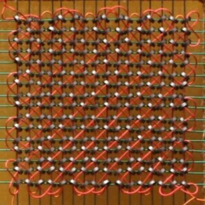
In ancient systems, volatile memories were built from vacuum tubes, ferrite cores (Figure 1), or transistor flip-flops. In modern systems, this role is served by Random Access Memory (RAM). This generally comes in two flavors, Static RAM (SRAM) and Dynamic RAM (DRAM), and most systems will contain both in various quantities to accommodate the performance, power, and size (both physical and logical) needs of the system.
For volatile memory of all types, confidentiality and integrity are the main security properties of concern. The ability of an attacker to maliciously read/write the contents has traditionally been the domain of software vulnerabilities such as memory safety issues. But we’ve seen the emergence of techniques that leverage hardware issues to achieve the same thing. Physical attacks are the most straightforward, especially when the hardware may be deployed in hostile environments (eg. edge computing), vulnerable to temporary access by an attacker (eg. a supply chain interdiction, or “evil maid“), or whenever the device may be easily lost, stolen, or confiscated (as in the case of mobile devices). Many of these known vulnerabilities are also exploitable by a local attacker on the system who may attempt to escalate privileges, and some of these are even exploitable remotely over the network.
In all cases, the solutions typically involve encrypting data (preferably using non-malleable ciphers, though this is uncommon for performance reasons), however performance overhead is an oft-cited concern unless the memory controller implements the encryption in hardware. You also need a safe place to store your memory encryption keys, which can itself be a challenge (typically solved by generating and storing the key within the SoC and accessible only to the memory controller itself). For microcontrollers with built-in RAM, directly accessing the bus is a much harder challenge for an attacker; however, many such devices have other ways to access the internal memories through debug functionality, which brings a new set of security concerns related to access control.
SRAM
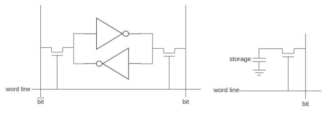
A typical single SRAM cell consists of six transistors (Figure 2): a pair of inverters arranged in a feedback loop to store a value, and gated connections to the row and column lines for reading and writing. This allows each cell to be addressed individually and quickly, but consumes energy the entire time the cell is powered, and takes up more area on a silicon die than a DRAM memory cell. Its use is most often limited to high speed memories within an SoC or microcontroller (caches, and other internal RAMs) and it is often sized in kilobytes or megabytes.
The startup value of an SRAM cell will contain a bias due to the unstable balanced nature of the inverter feedback loop (i.e. whichever inverter powers up faster will win). This bias is somewhat random and can be exploited to develop a useful physically unclonable function (PUF) on which to build higher level security features. The bias can however, be altered by ionizing radiation and annealing. This can affect the security guarantees of a PUF. Annealing can also be dependent on the current state of the SRAM. This may allow an attacker to effectively freeze the current SRAM contents, and similar to a cold boot attack on DRAM (discussed below), allow an attacker to recover its contents at a later time.
Intentionally causing bit-flips within memory can be achieved through a variety of advanced techniques including voltage and clock glitching, electromagnetic pulses (EMP), optical fault injection using infrared lasers, and various forms of ionizing radiation. All of these have the effect of altering data, and if done carefully could alter the behavior of the system in ways that are desirable to the attacker. Frequently, the attacker’s goal is to subvert a low-level security control, such as secure boot, debug re-enablement, or a vital authentication scheme.

DRAM
A DRAM cell consists of a single capacitor (Figure 2) which can passively (i.e. without power) store an amount of charge (an analog value enabling multiple bits per cell), and a single transistor to connect this to the row and column lines. While this simplicity offers much higher density (therefore higher storage capacity) and lower power than SRAM it comes with a number of tradeoffs. Parasitic leakage of charge into the substrate causes the stored value to degrade over time (on the order of seconds). This is overcome by periodically refreshing the stored values on every cell, a necessary interruption which can limit the performance of the overall system. Similarly, the simple design requires that all cells in a row be read together as a stream, an operation which disturbs the stored charge, requiring that it be written back again. These performance impacts are most often remedied by pairing DRAM with a faster but smaller SRAM for caching purposes.
The tightly-packed nature of DRAM is also the cause of some serious security concerns. Crosstalk (electromagnetic interference) between rows within the extremely dense DRAM memory becomes a concern, and researchers have developed techniques for exploiting this called RowHammer and RAMBleed. These vulnerabilities allow a local attacker on the system or a remote attacker (see ThrowHammer/NetHammer variants) to write (RowHammer) and read (RAMBleed) memory that they do not have permission for by repeatedly accessing, or hammering, adjacent memory rows. Any system using DRAM is vulnerable (including Error Correction Code (ECC) memory), yet there is no 100% defense. The best defense strategy currently relies on detection of active rowhammer attacks with a targeted row refresh (TRR), but these are optional and not yet widely deployed. Many proof-of-concept demonstrations are publicly available and it is only a matter of time before we see these attacks being used by malware in the wild.
For physical attacks, the same interposers that enable engineers to investigate memory signal issues also allow an attacker easy access to the memory bus between the host processor and the memory. Cold Boot attacks exploit the relatively slow data decay when the DRAM memory is unpowered, and this time can be extended to minutes/hours using cold temperatures. Techniques have been developed to apply this attack even to soldered-down memories.
Hybrid Memory Cube (HMC) and High Bandwidth Memory (HBM)
HMC and HBM are sophisticated uses of DRAM technology that achieve much higher performance for memory intensive applications, primarily through reduced latency and higher parallelism. Importantly for security, these devices contain additional controller elements (with yet more complex firmware) that must be robust and secured from attackers.
Non-Volatile Memory Technologies
Non-volatile memory stores the data and code persistently when the power is off. These come in an even wider array of options. Historically, various forms of magnetic media were used, including tapes, floppy disks, and spinning hard drives. These all require mechanical components which themselves are subject to normal wear and failure. Malicious wear can cause Denial-of-Service attacks in all types of persistent memory.
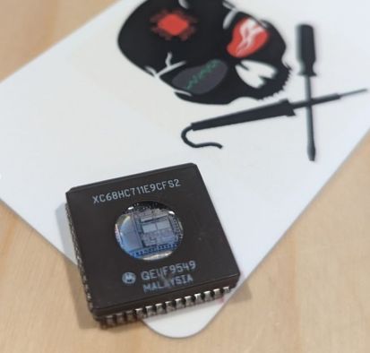
Solid state devices have some distinct advantages with respect to performance, power, and mechanical reliability. These devices are mostly based on storing charge using various microscopic semiconductor cell designs. Read-only Memory (ROM) comes in a number of forms and is often programmed during semiconductor fabrication. It is of limited utility in applications with dynamic content. Programmable ROM (PROM) allows a single programming operation to occur (eg. by an OEM device maker) and is otherwise similar to ROM. Erasable PROM (EPROM) are slightly more versatile in that they can be erased by UV light and reprogrammed which allows some level of manual field upgradeability. Electrically erasable PROM (EEPROM) and flash memory are fully in-circuit erasable due to the use of internal charge pumps and other devices. Flash memory is the most common solid state device you will find in almost all modern electronics.

From a security perspective, non-volatile memories have all the same concerns with bus access as does RAM, but they are more pronounced because of the lower pin count and lower speeds. This makes it easier for an attacker to access without expensive equipment. Moreover, thanks to the persistent nature of the memory, you have additional attacks to worry about:
- Offline (or “chip-off”) attacks, like cold-boot attacks on RAM, are where the memory is simply removed from the device and read/modified using an off-the-shelf flash reader, an operation that takes only minutes for practiced hands.
- Denial of service attacks due to malicious premature wear. Modern flash devices are only rated for 10k (or fewer!) erase cycles before they need replacement. When embedded in a product rather than say a removable micro-SD card, this can be devastating.
- NAND (very common) flash technology achieves great density but suffers from expected failure rates, and so requires bad block management and wear leveling algorithms. Commonly this functionality is implemented within a small microcontroller within the memory chip itself (eMMC and UFS) or within a companion storage controller chip (as in SSDs and NVMe drives). This frees the host operating system from having to tame these complexities. However, this modular design introduces exploitable data remanence concerns, and you may not know if data that should be erased is actually erased, which may lead to privacy concerns. JEDEC introduced the Secure Trim and Secure Erase commands in the eMMC 4.4 specification to help overcome this problem, however these are often slow and remain unused in the majority of embedded systems.
- Even when the secure erase functionality is used correctly, data might still be recoverable due to analog threshold effects. NIST provides media sanitization guidance that’s applicable to flash memory as well as magnetic media, and of course, physical destruction is effective.
- Ordinarily flash devices are intended to be erased in blocks of a particular size (tens or hundreds to kilobytes at a time). EEPROM and EPROM devices are similarly intended to be erased as a whole unit. Systems that rely on these properties might be vulnerable to abuse when smaller regions, even single bytes, are selectively erased, which might for example, allow the bypass of some security features.
- Finally, when the flash reaches end-of-life, its behavior is completely implementation defined. Some flash manufacturers choose to simply freeze the contents in place as a permanent record with no capability to erase, requiring physical destruction of the chips by security conscious users.
RPMB
Some memories (eMMC, UFS, SD, NVMe) can include a Replay Protected Memory Block (RPMB). This special data partition cannot be written or modified without knowledge of the provisioned secret key. Read protection can be further provided by encrypting the data. The secret key must be known to the host SoC and stored safely. It must be programmed into the memory chip (usually by the host firmware on first boot) in a secure environment because this operation itself is vulnerable to snooping. A common attack is to replace a provisioned memory chip with a new blank part, which may cause a careless host to provision the blank part with the same RPMB secret used on the original memory part, thus revealing it to the attacker. The SoC must treat the provisioning operation as a one-time event to avoid this.
Hybrid and Exotic Memory Technologies
It’s worth discussing a few other related technologies that do not cleanly fit into the above categories.
Battery-Backed RAM
RAM is sometimes used as non-volatile storage, in concert with a small battery or supercapacitor to provide power for data retention. This is frequently seen in applications such as:
- A part of a tamper detection system for security sensitive devices. These systems must be able to defend themselves from an attacker even when the main system power has been cut. Securing the backup power supply to the memory may be very important to the operation of the anti-tamper subsystem, and it therefore needs to be carefully designed to be within the anti-tamper envelope itself.
- Always-on-power (AOP) domains within a microcontroller. Most microcontrollers and SoCs implement low power features that let the bulk of the chip go to sleep and save power, while only a tiny portion of the system remains powered in order to resume without a full boot cycle. This functionality is supported by a small low-power SRAM used to retain system state across sleep/resume operations. For performance reasons a resume operation does not perform the extensive security validations (such as secure boot) that a full system boot would. Therefore it is vital that an attacker not be able to directly write the AOP RAM state, thus tricking a device into performing a resume from sleep rather than a full boot operation.
One-Time-Programmable Fuses
Modern SoC devices contain a number of security and other configuration options that are programmed only once. These typically come in some form of OTP memory, or “fuses”, and number in the tens or hundreds of bits. Most often these are set during device manufacturing, but in some situations it may be desirable to program them in the field (for say, software roll-back prevention). These fuses can be used for any number of purposes, but common uses include disabling of security-compromising debug interfaces, enabling hardware and firmware security features such as Secure Boot, and storage of sensitive encryption keys (for use with RPMB or RAM encryption).
Attacks against the fuses most often target the software that makes use of the fuses (through fault injection, side channel leakage, or software vulnerabilities), but there are some interesting vulnerabilities that (depending on the design) may affect the fuse arrays themselves. Two examples to highlight this:
- Under certain conditions, programmed (“blown”) fuses can regrow, thus putting the system into a typically less-secure state. Such behavior is likely to require either privileged access to the software environment, or physically invasive techniques, and so might be of a lower concern, depending on the system threat model.
- Certain SoCs are designed with a separate power input for the fuse banks. This allows an external attacker with only circuit-level access to selectively control the power to the fuse banks, thereby selectively cutting the power at carefully chosen intervals to “zero-out” fuses as they are read by the hardware and firmware.
Phase Change Memory
Phase change memory uses a variety of novel materials to provide the performance characteristics of RAM with the power and non-volatility of flash memory. From a security perspective, (some of) these memories have useful properties that might be useful. In particular, the data is often erased with heat, a generally undesirable property, but which could be used as an anti-tamper mechanism to react to certain physical attacks (in particular hot-air rework). Unfortunately, while the technology has been under development for many decades, it remains a topic of intense research, with no parts currently available in commercial volumes.
Final Thoughts
Almost all modern memory devices themselves contain computing elements, microcontrollers, and firmware to tame the complexities of modern interfaces and the complicated physics of the memory technology itself. Link training, wear leveling, caching, sleep and power management, manufacturing-related test functionality, are just some examples of these complexities. This functionality is backed by deeply-embedded firmware within the memory controller. This firmware is frequently written in the C language, where memory safety concerns pose a significant risk. These concerns increase as the firmware complexity increases, driven by modern memory protocols (such as NVMe) becoming increasingly complicated.
For memory vendors, understanding your target markets can be challenging; these are generic components and the final application and threat model is not always clear. Design for the worst case threat model, and defend against as many attacks as commercially viable. Firmware for memory controller components must be free of software defects. A robust and secure SDLC program including static analysis, security testing, and 3rd party audits can help.
We encourage device manufacturers and OEMs to probe their memory vendors. These vendors should have a good explanation as to how they avoid vulnerabilities in the vital firmware that will be deployed deep within the system. They need to have a coherent plan to maintain this firmware with ongoing security patches throughout the lifetime of a product.
When designing the system, think deeply about how an attacker might exploit the system’s memory interfaces, and design in countermeasures wherever possible. Memory encryption, careful key provisioning and management, and the selection of SoC and memory components that support the security guarantees are extremely important to get right at the earliest stages of product development.
